- 您现在的位置:买卖IC网 > Sheet目录3889 > PIC16F1827-I/SS (Microchip Technology)IC PIC MCU FLASH 4K 20-SSOP
216
2570N–AVR–05/11
ATmega325/3250/645/6450
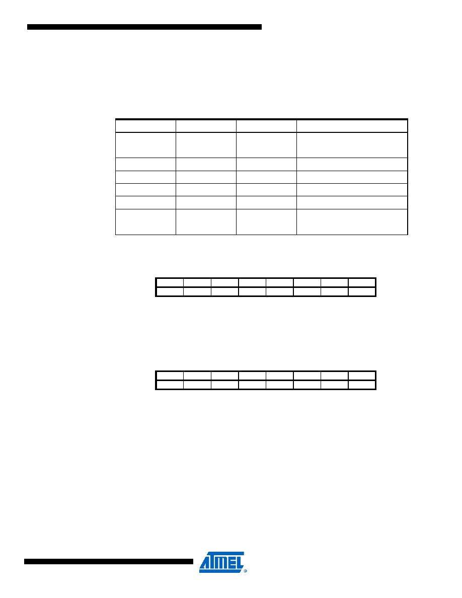
Bits 2:0 – ADPS2:0: ADC Prescaler Select Bits
These bits determine the division factor between the XTAL frequency and the input clock to the
ADC.
23.8.3
ADCL and ADCH – The ADC Data Register
ADLAR = 0
ADLAR = 1
When an ADC conversion is complete, the result is found in these two registers. When ADCL is
read, the ADC Data Register is not updated until ADCH is read. Consequently, if the result is left
adjusted and no more than 8-bit precision is required, it is sufficient to read ADCH. Otherwise,
ADCL must be read first, then ADCH.
The ADLAR bit in ADMUX, and the MUXn bits in ADMUX affect the way the result is read from
the registers. If ADLAR is set, the result is left adjusted. If ADLAR is cleared (default), the result
is right adjusted.
Table 23-5.
ADC Prescaler Selections
ADPS2
ADPS1
ADPS0
Division Factor
00
0
2
00
1
2
01
0
4
01
1
8
10
0
16
10
1
32
11
0
64
11
1
128
Bit
151413121110
9
8
–
ADC9
ADC8
ADCH
ADC7
ADC6
ADC5
ADC4
ADC3
ADC2
ADC1
ADC0
ADCL
765
4321
0
Read/Write
RRRR
Initial Value
000
0000
0
000
0000
0
Bit
151413121110
9
8
ADC9
ADC8
ADC7
ADC6
ADC5
ADC4
ADC3
ADC2
ADCH
ADC1
ADC0
–
––––
–
ADCL
765
4321
0
Read/Write
RRRR
Initial Value
000
0000
0
000
0000
0
发布紧急采购,3分钟左右您将得到回复。
相关PDF资料
PIC12C508-04/P
IC MCU OTP 512X12 8DIP
22-15-3153
CONN FFC/FPC 15POS .100 RT ANG
PIC16F1826-I/MV
IC PIC MCU FLASH 2K 28-UQFN
PIC16F1825-I/P
MCU PIC 14K FLASH 1K RAM 14DIP
22-02-3153
CONN FFC/FPC VERTICAL 15POS .100
22-15-3143
CONN FFC/FPC 14POS .100 RT ANG
22-02-3143
CONN FFC/FPC VERTICAL 14POS .100
502078-2110
CONN FPC .25MM 21POS R/A SMD
相关代理商/技术参数
PIC16F1827T-I/ML
功能描述:8位微控制器 -MCU 7KB Flash 384 byte 32 MHz Int. Osc RoHS:否 制造商:Silicon Labs 核心:8051 处理器系列:C8051F39x 数据总线宽度:8 bit 最大时钟频率:50 MHz 程序存储器大小:16 KB 数据 RAM 大小:1 KB 片上 ADC:Yes 工作电源电压:1.8 V to 3.6 V 工作温度范围:- 40 C to + 105 C 封装 / 箱体:QFN-20 安装风格:SMD/SMT
PIC16F1827T-I/MQ
功能描述:8位微控制器 -MCU 7KB Flash 384 byte 32 MHz Int. Osc RoHS:否 制造商:Silicon Labs 核心:8051 处理器系列:C8051F39x 数据总线宽度:8 bit 最大时钟频率:50 MHz 程序存储器大小:16 KB 数据 RAM 大小:1 KB 片上 ADC:Yes 工作电源电压:1.8 V to 3.6 V 工作温度范围:- 40 C to + 105 C 封装 / 箱体:QFN-20 安装风格:SMD/SMT
PIC16F1827T-I/MV
功能描述:8位微控制器 -MCU 7KB Flash 384 RAM RoHS:否 制造商:Silicon Labs 核心:8051 处理器系列:C8051F39x 数据总线宽度:8 bit 最大时钟频率:50 MHz 程序存储器大小:16 KB 数据 RAM 大小:1 KB 片上 ADC:Yes 工作电源电压:1.8 V to 3.6 V 工作温度范围:- 40 C to + 105 C 封装 / 箱体:QFN-20 安装风格:SMD/SMT
PIC16F1827T-I/SO
功能描述:8位微控制器 -MCU 7KB Flash 384 byte 32 MHz Int. Osc RoHS:否 制造商:Silicon Labs 核心:8051 处理器系列:C8051F39x 数据总线宽度:8 bit 最大时钟频率:50 MHz 程序存储器大小:16 KB 数据 RAM 大小:1 KB 片上 ADC:Yes 工作电源电压:1.8 V to 3.6 V 工作温度范围:- 40 C to + 105 C 封装 / 箱体:QFN-20 安装风格:SMD/SMT
PIC16F1827T-I/SS
功能描述:8位微控制器 -MCU 7KB Flash 384 byte 32 MHz Int. Osc RoHS:否 制造商:Silicon Labs 核心:8051 处理器系列:C8051F39x 数据总线宽度:8 bit 最大时钟频率:50 MHz 程序存储器大小:16 KB 数据 RAM 大小:1 KB 片上 ADC:Yes 工作电源电压:1.8 V to 3.6 V 工作温度范围:- 40 C to + 105 C 封装 / 箱体:QFN-20 安装风格:SMD/SMT
PIC16F1828-E/ML
功能描述:8位微控制器 -MCU 7 KB Flash 256b RAM 32 MHz Int. Osc RoHS:否 制造商:Silicon Labs 核心:8051 处理器系列:C8051F39x 数据总线宽度:8 bit 最大时钟频率:50 MHz 程序存储器大小:16 KB 数据 RAM 大小:1 KB 片上 ADC:Yes 工作电源电压:1.8 V to 3.6 V 工作温度范围:- 40 C to + 105 C 封装 / 箱体:QFN-20 安装风格:SMD/SMT
PIC16F1828-E/P
功能描述:8位微控制器 -MCU 7 KB Flash 256b RAM 32 MHz Int. Osc RoHS:否 制造商:Silicon Labs 核心:8051 处理器系列:C8051F39x 数据总线宽度:8 bit 最大时钟频率:50 MHz 程序存储器大小:16 KB 数据 RAM 大小:1 KB 片上 ADC:Yes 工作电源电压:1.8 V to 3.6 V 工作温度范围:- 40 C to + 105 C 封装 / 箱体:QFN-20 安装风格:SMD/SMT
PIC16F1828-E/SO
功能描述:8位微控制器 -MCU 7 KB Flash 256b RAM 32 MHz Int. Osc RoHS:否 制造商:Silicon Labs 核心:8051 处理器系列:C8051F39x 数据总线宽度:8 bit 最大时钟频率:50 MHz 程序存储器大小:16 KB 数据 RAM 大小:1 KB 片上 ADC:Yes 工作电源电压:1.8 V to 3.6 V 工作温度范围:- 40 C to + 105 C 封装 / 箱体:QFN-20 安装风格:SMD/SMT